
A Pnp Bipolar Transistor is a three-layer semiconductor device designed to control current. Its structure contains a P-type emitter, an N-type base, and a P-type collector. The arrangement seems simple, yet its operation depends on careful voltage relationships. In practical circuits, engineers use PNP devices for high-side switching, signal amplification, and current sourcing.
As transistor pioneer William Shockley explained, “A transistor is a device for amplifying electrical signals.” That statement captures the central idea, although it does not reveal the full behavior of a PNP device. When the emitter sits at a higher potential than the base, the emitter-base junction becomes forward biased. A small base current then helps control a larger collector current. Conventional current flows from the emitter toward the collector. Electron movement follows the opposite direction.
The differences become clearer on a workbench. A PNP transistor may switch a relay when its base voltage falls below the emitter voltage. A multimeter can confirm its junction behavior, but measurements may change with temperature, load, and transistor type. Datasheets also matter. Pin layouts are not universal, and incorrect assumptions can damage the component. This is where many beginner explanations become too neat. Real circuits include leakage, saturation, voltage limits, and heat. Understanding those imperfections makes the Pnp Bipolar Transistor easier to select, test, and apply safely. The sections ahead examine its construction, operating principle, symbols, biasing methods, and practical circuit behavior.
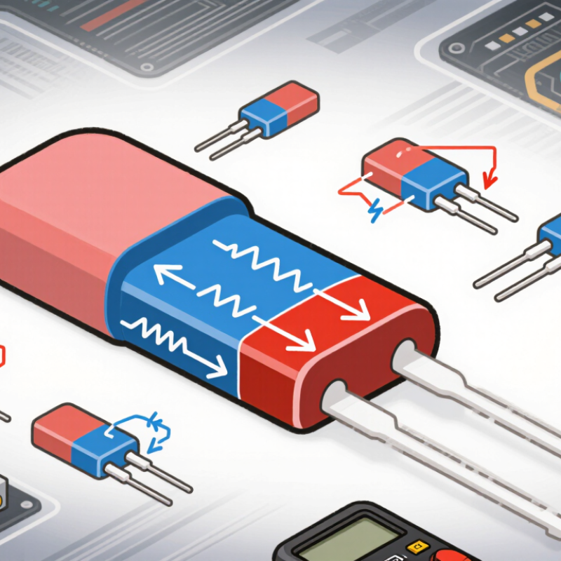
A PNP bipolar transistor is a three-layer semiconductor device with a P-type emitter, an N-type base, and a P-type collector. Its basic structure is written as P-N-P. The emitter injects charge carriers, while the collector gathers them. The base controls this movement with a small current.
In normal active operation, the emitter sits at a higher voltage than the base. A silicon PNP transistor usually needs about 0.6 to 0.7 volts between these terminals. Conventional current then flows from emitter to collector. The circuit symbol shows an arrow pointing inward, toward the base. This detail is easy to forget during bench testing. A reversed part may appear dead.
The base is intentionally thin and lightly doped. That design allows most injected carriers to cross it. The collector is usually larger, helping it handle heat and voltage. Real devices rarely behave so neatly. Temperature, leakage current, and saturation can change the readings. The World Semiconductor Trade Statistics 2024 forecast placed global semiconductor sales at about 611 billion US dollars, showing the scale of the wider device industry. However, that report does not separate PNP transistor sales. This limitation matters when interpreting market claims. In practical circuits, engineers still check the datasheet, measure terminal voltages, and allow for variation instead of trusting the ideal 0.7-volt rule.
| Data Dimension | PNP Bipolar Transistor Information | Practical Significance |
|---|---|---|
| Device category | Bipolar junction transistor (BJT) | Uses both majority and minority charge carriers to control current. |
| Terminal structure | Emitter, base, and collector | The base controls the larger current flowing between the emitter and collector. |
| Semiconductor layers | P-type emitter, N-type base, and P-type collector | The P-N-P arrangement determines the device polarity and carrier movement. |
| Majority carriers | Holes | Holes are injected from the emitter toward the base and collector during normal operation. |
| Base characteristic | Thin and lightly doped N-type region | A thin base allows most injected holes to pass through to the collector. |
| Emitter characteristic | Heavily doped P-type region | Provides a strong supply of holes for transistor action. |
| Collector characteristic | Moderately doped P-type region, usually physically larger than the emitter | Collects carriers and dissipates heat while supporting the applied voltage. |
| Normal active bias | Emitter-base junction forward-biased; collector-base junction reverse-biased | This bias condition enables amplification. |
| Typical silicon turn-on voltage | Approximately 0.6–0.7 V from base to emitter in forward operation | For a PNP device, the emitter is typically about 0.6–0.7 V more positive than the base. |
| Conventional current direction | From emitter to collector through the transistor | Current flows from a higher potential at the emitter toward a lower potential at the collector. |
| Base-current relationship | IE = IC + IB | The emitter current equals the sum of collector current and base current. |
| Common-emitter current gain | β or hFE = IC / IB; the value depends on the device and operating conditions | A small base current can control a substantially larger collector current. |
| Cutoff region | Both junctions are not forward-biased; collector current is very small | Used to represent the OFF state in switching circuits. |
| Active region | Emitter-base junction is forward-biased and collector-base junction is reverse-biased | Used for linear voltage or current amplification. |
| Saturation region | Both junctions are forward-biased | Used to represent the ON state, although the transistor no longer provides normal linear amplification. |
| Circuit-symbol arrow | The emitter arrow points inward toward the base | The inward arrow distinguishes a PNP transistor from an NPN transistor. |
| Common applications | High-side switching, signal amplification, current-source circuits, and analog control stages | Useful when the load is connected below a positive supply and should be switched from the high side. |
| Key design consideration | The base must be driven sufficiently below the emitter for forward operation | Incorrect base-emitter polarity can prevent conduction or damage the device if voltage limits are exceeded. |
What Is a PNP Bipolar Transistor and How Does It Work?
How the PNP Transistor’s Three Semiconductor Layers Work
A PNP bipolar transistor contains three semiconductor layers: p-type emitter, n-type base, and p-type collector. The emitter supplies holes, which are positive charge carriers. It is heavily doped for efficient injection. The base is extremely thin and lightly doped. This design lets most holes cross it without recombining. The collector receives these carriers and controls heat during operation.
The device turns on when its emitter is more positive than its base. In a silicon transistor, the required base-emitter difference is commonly near 0.6 to 0.7 volts. A lower base voltage allows holes to move from emitter to collector. Conventional current flows toward the collector, while base current controls the larger collector current. The relationship is often expressed as IC ≈ βIB, although β changes with temperature, voltage, and manufacturing variation.
Real measurements are less tidy.
IEC 60747-5-2 provides standardized terminology and test guidance for bipolar transistors. Industry forecasts also show why these devices remain relevant. The World Semiconductor Trade Statistics forecast global semiconductor sales of about 697 billion dollars in 2025. That broad market includes many transistor types, not only PNP devices. On a workbench, leakage current can rise noticeably as temperature increases. The simple three-layer picture therefore needs caution. Package resistance, saturation, and switching speed can alter expected behavior. A PNP transistor is not merely an inverted NPN transistor; its carrier movement and circuit reference directions require careful checking.
A PNP bipolar transistor uses a positive emitter, negative base, and positive collector structure. Its current flow can seem backward at first. When the emitter sits about 0.6–0.7 volts above the base, the emitter-base junction becomes forward biased. Holes then move from the p-type emitter into the thin n-type base. A smaller portion recombines with electrons there, creating base current. Most holes cross the base and reach the collector. Conventional current therefore travels from emitter to collector, while electron movement runs in the opposite direction.
For example, an emitter at +5 volts and a base near +4.3 volts may turn the device on. The control current leaves the base terminal in a PNP circuit. This detail is often missed in quick diagrams.
In active operation, a small base current controls a much larger collector current. The exact ratio depends on temperature, device construction, and operating point. The 2023 International Roadmap for Devices and Systems report highlights tighter power and charge-control demands in advanced electronics. Meanwhile, the World Semiconductor Trade Statistics reported 2024 semiconductor sales of about 626.9 billion dollars, showing the scale of systems relying on controlled charge movement.
Tips: Check voltage polarity before checking current direction. Do not treat holes as empty spaces only; they represent mobile positive charge. A water-flow analogy helps briefly, but it can hide recombination and carrier movement. Measure emitter-base voltage under load, because assumptions can be wrong.
What Is a PNP Bipolar Transistor and How Does It Work?
Biasing determines whether a PNP bipolar transistor switches, amplifies, or remains inactive. Its emitter usually sits at the highest voltage in the circuit. The base must be slightly lower than the emitter to forward-bias the emitter-base junction. For a silicon device, this difference is often about 0.6 to 0.7 volts. The collector remains at a lower voltage, allowing conventional current to move from emitter to collector.
Small base-current changes can control a much larger collector current. This behavior makes the PNP transistor useful in high-side switching and signal amplification. In the forward-active region, the emitter-base junction is forward biased, while the collector-base junction is reverse biased. If the base rises too close to the emitter, the transistor approaches cutoff. If the base falls too far, the device may enter saturation.
The 0.7-volt rule is practical, but imperfect. Temperature, current, and transistor construction change the actual voltage. A reliable circuit therefore uses measured values and a defined bias network, not assumptions alone. On a workbench, checking emitter, base, and collector voltages can reveal incorrect polarity quickly. I have found that many apparent transistor faults are really biasing errors. A floating base is a warning sign. Careful resistor selection also limits base current and reduces thermal stress. Biasing is not merely a setup step; it establishes the operating conditions that make PNP behavior predictable.
A PNP bipolar transistor uses holes as its main charge carriers. Its emitter normally connects to the positive supply, while the base controls current flowing toward the collector. For a silicon device, the base usually needs to sit about 0.7 volts below the emitter for conduction. Small voltage changes can control a much larger collector current. That relationship makes the PNP transistor useful in both switching and amplification.
The common-emitter configuration is widely used for high-side switching. A load connects between the collector and ground, and pulling the base lower turns the transistor on. This arrangement can control relays, indicator lamps, and power rails when the load current stays within the rated limits. A resistor in the base path remains important. Without it, excessive base current can damage the device.
In the common-collector configuration, the collector connects to the positive rail, and the output appears at the emitter. This emitter follower provides current gain and a lower output resistance, making it useful for buffering sensor signals or driving another circuit. The output typically stays about 0.7 volts below the base.
The common-base configuration offers low input resistance and useful high-frequency behavior, although it is less familiar in basic designs.
I have found high-side switching intuitive after checking voltage polarity with a meter. The simple rule is useful, but not complete. Leakage, heat, saturation, and load transients still deserve careful testing.


